











Material Properties and Applications of PDMS Membrane Sensing Chips
I. Core Material Properties of PDMS Membranes for Sensing Chip Integration
1. Mechanical Properties (Core for Tactile / Pressure Sensing)
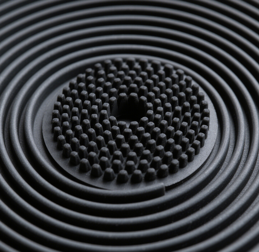
Microstructurability: Molding can replicate pyramid patterns, micropores, wrinkles and fingerprint microprotrusions to drastically boost pressure sensing sensitivity. Ultra-thin membranes (50–500 μm) deliver millisecond-scale deformation response.
2. Optical Properties (Mandatory for Optical Sensing Chips)
3. Biochemical and Interfacial Properties (For Biosensing Chips)
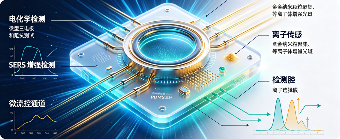
PDMS Thin-Film Sensing Chips
Non-cytotoxic and biocompatible, suitable for direct skin attachment or in-vivo implantation. Air, water and oxygen permeable, meeting requirements for cell culture and in-situ detection of sweat/body fluids.
Intrinsically hydrophobic; surface modification via oxygen plasma or Pluronic converts it to hydrophilicity to enable self-driven fluid flow in microfluidics. Au/Ag thin films can be sputtered on PDMS to fabricate flexible electrodes featuring high peel strength and stable conductivity under stretching.
4. Fabrication and Packaging Advantages
5. Tunable Permeation Properties (For Gas / Ion Sensing)
II. Segmented Applications of PDMS Membranes in Various Electronic Sensing Chips
(I) Flexible Pressure / Tactile Sensing Chips (Electronic Skin, E-skin) — The Most Dominant Application
Capacitive Tactile Chips
Typical solution: GaN optoelectronic tactile chips coated with fingerprint-patterned PDMS films that mimic human epidermis, applied to organ tactile detection in minimally invasive surgery and sensor arrays for precision robotic grasping.
Structure of PDMS Bionic Tactile Chips
Piezoresistive Sensing Chips
Encapsulation Protective Layer
(II) Microfluidic Biochemical Sensing Chips (Lab-on-Chip, Sweat / Body Fluid Detection)
Fluid Channel Layer
Stacked Structure of PDMS Microfluidic Sweat Sensing Chips
Separation / Breathable Diaphragm
Encapsulation of Implantable On-Chip Electrodes
(III) Gas / VOC Sensing Chips (Fiber Optic, MOS, Electrochemical Gas-Sensitive Chips)
Fiber-Optic SPR/VOC Chips
Protective Membranes for Metal Oxide Semiconductor (MOS) Gas-Sensitive Chips
Breathable Diaphragms for Electrochemical Gas Sensors
(IV) Optoelectronic / SPR / SERS Optical Sensing Chips
Flexible Optical Substrates
Sealing Layers for SERS Enhancement Cavities
(V) Wearable Physiological Electrical Sensing Chips (ECG, EMG, EEG)
Flexible Substrates
Ion Channel Buffer Layer
III. Standard Fabrication of PDMS Films and Chip Integration Processes
Film Preparation
Film Forming Methods
- Spin-coating: 500–3000 rpm, film thickness 10–200 μm with high uniformity, compatible with wafer-level sensing chips;
- Blade-coating / Casting: Molded thick films (200 μm–2 mm) for microfluidic channels and tactile dielectric layers;
- Dip-coating: Ultra-thin gas-sensitive coatings on fiber end faces.
Curing Conditions
- Complete crosslinking: Baking at 60–65 °C for 2 h;
- Fast curing: 110 °C for 1.5 h;
- Slow room-temperature curing (24 h): Delivers higher film elasticity.
Chip Bonding (Core Integration Step)
Surface Modification for Functional Expansion
- Oxygen plasma: Convert hydrophobic surface to hydrophilicity for self-driven microfluidic flow;
- Gold / titanium sputtering: Fabricate on-chip flexible electrodes;
- Parylene vapor deposition: Form dense waterproof barriers to resolve water absorption drift of implanted devices;
- Conductive filler doping: Manufacture piezoresistive elastic sensing films.
IV. Inherent Technical Limitations and Chip-Level Optimization Strategies
1. Intrinsic Drawbacks
- Inherent hydrophobicity tends to adsorb organic substances, causing non-specific adsorption interference in biochemical detection;
- Water vapor and polar small molecules readily permeate PDMS, leading to film swelling and sensing baseline drift under high temperature or long-term immersion;
- Low insulating dielectric constant (ε ≈ 2.7) caps the maximum sensitivity of pure PDMS capacitive sensors;
- Poor resistance to strongly polar solvents (acetone, high-concentration ethanol), causing swelling and deformation of microfluidic organic detection channels.
2. Engineering Optimization Solutions
- Composite modification: Dope PDMS with high-dielectric BaTiO₃ particles to boost capacitive sensing sensitivity; porous/Parylene composite double-layer films block moisture penetration;
- Surface functionalization: Pluronic and hydrophilic coatings reduce protein adsorption;
- Ratio regulation: Increase curing agent proportion to raise crosslink density and mitigate swelling;
- Composite encapsulation: PDMS + PI / epoxy composite layers balance flexibility and barrier performance for industrial and implantable high-precision sensing chips.
V. Industrial Application Scenarios and Development Trends
Application Scenarios
- Healthcare & Medical: Wearable sweat biochemical patches, tactile sensors for minimally invasive surgery, implantable intracranial pressure monitoring chips, flexible ECG electrodes;
- Robotics & Human-Machine Interaction: Electronic skin tactile arrays, force perception chips for bionic manipulators;
- Environmental Monitoring: Miniature fiber-optic VOC sensors, portable toxic gas detection chips;
- Biological Laboratories: Organ-on-Chip cell microfluidic sensing, high-throughput biochemical detection chips;
- Consumer Electronics: Curved screen touch sensing, flexible wristband pressure & pulse detection chips.
Future Development Directions
- Functionally integrated PDMS: Monolithic conductive, gas-sensitive and ion-selective thin films enabling simultaneous multi-parameter detection on single chips;
- Ultra-thin nanoscale PDMS coatings for miniature MEMS and chip-scale packaged micro gas-sensitive devices;
- Degradable modified PDMS for disposable short-term implantable sensing chips to avoid secondary surgical removal;
- Large-area roll-to-roll mass production of PDMS flexible sensor arrays to cut commercialization costs of wearable chips;
- High-barrier composite PDMS films to address long-term stability bottlenecks of implantable and industrial high-temperature/high-humidity applications.