











Guide to Material Selection and Application of Thermal Interface Sheets and Electromagnetic Shielding Materials for LiDAR
hermal Interface Sheets and Electromagnetic Shielding Materials for LiDAR
I. Dedicated Thermal Interface Sheets for LiDAR (Thermal Interface Materials, TIM)
(I) Main Grades and Application Scenarios
- Low-volatility, low-oil thermal silicone sheet (mainstream for mass production)
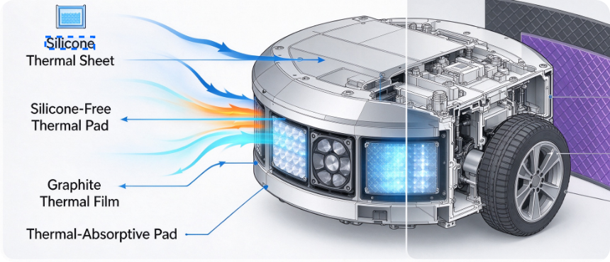
Fabricated with modified silicone matrix filled with high-thermal-conductivity alumina and aluminum nitride fillers, this is the most widely adopted thermal material for automotive LiDAR. Optimized formulations remove highly volatile D3/D4/D5 siloxane oligomers to drastically reduce oil bleed, preventing fogging of optical lenses and contamination-induced failure of photodetector chips.
- Silicone-free thermal pad (for optically sensitive zones)
Polyurethane/carbon fiber composite silicone-free substrate, containing zero silicone oil or siloxane molecules. It fundamentally eliminates contamination from silicone bleed-out. This dedicated thermal material is used for modules adjacent to short-range optical paths and optical windows, solving the industry pain point of optical-path contamination from trace volatiles of silicone sheets.
- Artificial graphite thermal film (for heat spreading)
Ultra-high in-plane thermal conductivity (1000~1800 W/mK), thin and flexible (thickness: 25~100 μm). Primarily used for full-area heat spreading on housings and PCB surfaces to eliminate hotspots. Through-plane thermal conductivity is low; only for planar heat spreading rather than gap filling.
- Integrated thermal-conductive and wave-absorbing pad (for high-density integrated designs)
Combines thermal conduction and high-frequency electromagnetic wave absorption. Covers interference bands from 500 MHz to 40 GHz. It simultaneously provides component cooling and local EMI suppression, saving limited internal space for compact, highly integrated solid-state LiDAR.
(II) Key Considerations for Thermal Sheet Application
- Optical isolation principle: All silicone-containing thermal sheets must maintain a safe clearance from optical lenses, optical paths and photodetector chips. Direct contact with optical zones is prohibited. Only silicone-free thermal pads can be deployed near optical paths.
- Thickness matching principle: Select thickness precisely based on assembly gaps. Optimal compression ratio is 20%~40%. Excessively small gaps cause squeeze-out; oversized gaps raise thermal resistance and lead to thermal failure.
- Automotive reliability: Must pass AEC-Q automotive qualification and low-outgassing tests to prevent volatile release under high temperature & humidity and long-term contamination of optical systems.
- Vibration compatibility: Prioritize high-resilience, low-stress grades. Prevent material fatigue, shifting or detachment under road vibration to sustain stable long-term thermal performance.
II. Electromagnetic Shielding Materials for LiDAR
(I) Main Grades and Application Scenarios
- Metal shielding can (board-level primary shielding)
Shielding cavities fabricated from 0.2 mm nickel silver, stainless steel or aluminum alloy. It is the mainstream shielding solution for core PCB circuits of LiDAR. It provides wideband shielding from DC up to tens of GHz with shielding effectiveness of 50~100 dB, meeting the safety certification requirement of minimum 60 dB isolation for automotive sensors.
- Conductive foam / conductive fabric (cavity gap shielding)
Polyurethane foam core clad with highly conductive nickel-copper plating. Flexible and compressible, suitable for assembly seams of LiDAR housings, wire harness interfaces and gaps between shielding cans, solving cavity electromagnetic leakage. Good resilience ensures sustained shielding sealing at gaps under vibration.
- High-frequency wave-absorbing material (stray wave suppression)
Flexible thin wave-absorbing sheets optimized for the primary 2 GHz~6 GHz interference band of LiDAR. Unlike reflective shielding materials, it converts stray electromagnetic waves into heat, eliminating secondary interference caused by reflection from shields and mitigating high-frequency resonance and crosstalk.
- Optically transparent conductive coating (window electromagnetic shielding)
ITO (Indium Tin Oxide) transparent coating deposited on LiDAR optical windows. It delivers high optical transmittance together with electromagnetic shielding. It does not interfere with 905 nm /1550 nm laser transmit/receive, while blocking external high-frequency electromagnetic waves from entering the cavity through the window.
(II) Key Considerations for Electromagnetic Shielding Material Application
- High-frequency priority: LiDAR interference is dominated by GHz-band signals. Low-frequency shielding materials shall not be used. High-frequency high-shielding-effectiveness grades must be selected to avoid shielding failure at high frequencies.
- Co-design of shielding and heat dissipation: Metal shielding cans shall reserve thermal paths or be paired with thermal sheets / thermal-conductive wave-absorbing materials. Avoid heat accumulation inside enclosed shielding cavities and conflicts between heat dissipation and EMC.
- Zero optical interference: Only ITO transparent conductive coating can be used for optical windows. Opaque shielding materials or conductive foam must not block optical paths, to prevent transmittance degradation and laser TX/RX loss.
- Full gap sealing: All assembly seams of housings, harnesses and shielding cans shall be fully covered with flexible shielding materials. Electromagnetic leakage mostly originates from gaps; partial gaps drastically degrade overall shielding effectiveness.
- Avoid secondary interference: Wave-absorbing materials are preferred inside high-frequency cavities to reduce superposition of reflected electromagnetic waves from metal shields, preventing signal distortion and excessive noise in point clouds.
III. General Principles for Coordinated Material Selection
- Optical path zone: Silicone-free thermal pad + ITO transparent shielding coating. Prevent silicone contamination, light obstruction and electromagnetic intrusion to preserve optical precision.
- Core chip zone: Low-volatility silicone thermal sheet + metal shielding can + local wave-absorbing material. Balances efficient heat dissipation, high-frequency shielding and stray-wave suppression.
- Cavity seam zone: Conductive foam + thin graphite thermal film. Achieves electromagnetic sealing and overall heat spreading, compatible with automotive vibration.
- Highly integrated compact models: Prefer integrated thermal-conductive wave-absorbing pads to simplify structure, save space and resolve heat dissipation and EMC concurrently.