


Treatment‑Free Conductive Substrate for Flexible Electronics Manufacturing – PDMS
2026/03/20
0
I. Industry Pain Point: Manufacturing Bottlenecks of Low Surface Energy Substrates

Treatment‑Free Conductive Substrate
In the field of flexible electronics, low surface energy substrates such as silica gel/PDMS are widely used in smart wearables, medical devices and other scenarios due to their light weight, flexibility and excellent biocompatibility. However, the challenge of conductive layer adhesion has long restricted industrial development:
Traditional solutions rely on pretreatment processes such as plasma treatment (equipment cost exceeding ten million US dollars, with maintenance costs accounting for 15%) and chemical modification (complex processes involving sulfuric acid/UV laser treatment);
The adhesion strength of the conductive layer on untreated substrates is only 0.37 MPa, and even after optimized treatment, the maximum value is merely 2.77 MPa, accompanied by issues such as substrate damage and environmental risks;
Multi-step pretreatment prolongs the production cycle by more than 30%, resulting in poor compatibility with large-scale production and a significant increase in manufacturing costs.
II. Core Innovation: Treatment-Free Breakthrough of SECrosslink Silver Paste Technology
Conductive PDMS films based on SECrosslink silver paste technology achieve a disruptive breakthrough through a dual mechanism of physical adsorption + chemical affinity:
- Core Treatment-Free Principle: Using high-purity silver powder as the conductive medium and a customized elastomer resin system, stable chemical bonding and molecular-level adsorption are formed with the silica gel/PDMS surface during curing. No pretreatment steps such as plasma or chemical etching are required, enabling direct adaptation to substrate surface properties.
- Scalability Compatibility: Compatible with mainstream processing methods such as screen printing and blade coating. Its low-temperature rapid curing feature (≤120℃, curing time < 30 minutes) allows seamless integration into existing flexible electronics production lines, realizing mass production without equipment modification.
III. Technical Support: Quantitative Performance and Standard Verification
All key indicators reach top industry levels and have passed dual verification of national standards and actual working conditions:
- Adhesion meets GB/T 9286-98 Grade 5B: The cut edges are completely smooth with no peeling in cross-cut tests (equivalent to ASTM D3359-17 Grade 5B), far exceeding the adhesion performance of traditional treatment technologies and completely eliminating peeling risks.
- Ultimate Mechanical Durability: After 1000 cycles of 100% tensile stretching, the conductive layer shows no edge lifting or cracking, with a resistance change rate below 50 Ω, fully meeting the requirements of dynamic scenarios such as human movement and equipment deformation.
- Metal-Grade Conductivity: Volume resistivity as low as 10⁻⁵ Ω·cm, close to the conductivity of pure silver (pure silver resistivity: 1.59×10⁻⁶ Ω·cm), far superior to flexible conductive materials such as silver nanowires (10–50 Ω/□) and graphene (10–100 Ω/□).
- Environmental Friendliness and Safety: Adopts an eco-friendly solvent system, avoiding substrate corrosion and pollutant emissions caused by chemical pretreatment, ensuring biosafety for medical and wearable devices.
IV. Differentiating Advantages: Simplified Processes and Cost Revolution
| Comparison Items | Traditional Technology (Including Pretreatment) | SECrosslink Treatment-Free Technology |
|---|---|---|
| Process Steps | Substrate cleaning → Surface modification → Conductive layer printing → Curing (4–6 steps) | Direct printing → Curing (2 steps) |
| Equipment Investment | Requires plasma/chemical treatment equipment (ten-million RMB level) | Compatible with existing printing equipment, zero additional investment |
| Production Cycle | Single batch ≥ 4 hours | Single batch ≤ 1 hour |
| Comprehensive Cost | High unit cost including pretreatment, main materials and energy consumption | Pretreatment costs eliminated, comprehensive cost reduced by 40%–60% |
| Substrate Compatibility | Prone to thermal deformation and performance degradation of PI/PET substrates | Non-damaging adaptation to the full range of silica gel/PDMS substrates |
The core differentiation lies in breaking the industry convention that “low surface energy substrates must undergo pretreatment”. Through interfacial interaction innovation, it achieves process simplification while ensuring performance, resolving the traditional technology dilemma of “unable to balance performance and cost”.
V. Application Scenarios: Empowering Flexible Electronics Innovation Across Multiple Fields
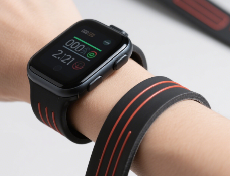
- Smart Wearable Devices: Directly printed on silica gel wristbands and flexible electrodes, adapting to 100% tensile deformation from human movement and ensuring long-term stability of conductive circuits.
- Medical Flexible Devices: Leveraging PDMS biocompatibility and treatment-free processes to manufacture wound monitoring patches and implantable electrodes, avoiding chemical residue risks.
- High-End Flexible Electronics: Flexible displays, automotive flexible sensors, microfluidic devices, etc., meeting requirements for light weight, portability and dynamic operation.
- Large-Scale Manufacturing: Supports large-area printing over 100 cm², compatible with various scalable processes such as inkjet and screen printing, with a stable yield rate above 98%.