


Application of PDMS in Robotic Electronic Skin
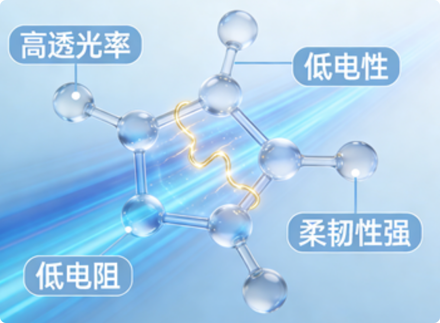
I. Characteristics of Conductive Films and Adaptability to Electronic Skin
II. Core Preparation Processes and Technical Key Points
Laser-Induced Vapor Deposition
By adjusting laser power and gas ratio, the packing density of conductive particles can be accurately controlled to tune the resistance to 100–200 kΩ, with excellent conductivity uniformity (no agglomeration).
Low-Temperature Solution Process
By controlling filler concentration (e.g., AgNWs at 0.5–1.2 mg/mL), the target resistance range can be stably obtained. This method features low cost and suitability for large-scale production; the relative resistance change remains < 5% after 1000 bending cycles.
Composite Conductive Hydrogel Method
Such conductive films combine adhesiveness and flexibility, with resistance precisely controllable at 150–200 kΩ, ideal for skin-adherent health-monitoring sensors.
III. Typical Application Scenarios and Technical Breakthroughs
1. Flexible Pressure-Sensing Electronic Skin
Conductive films in this resistance range enable a pressure sensing span of 0.0005–40 kPa, with a gauge factor (GF) of 10–50 and fast response time, allowing accurate recognition of varying pressure levels such as fingertip pressing and limb contact.
For example, electronic skin based on a CNT–TPU composite conductive film maintains stable performance after 11,000 pressing cycles, with resistance fluctuation < 3%.
Integration with interlocked micro-dome arrays can further enhance sensitivity (e.g., Sₚ = 184.82 kPa⁻¹), suitable for fine-operation feedback in minimally invasive surgical robots.
2. Human Health Monitoring Systems
-
Respiration monitoring:
Ultra-thin conductive films (near 0 μm thickness) of 100–200 kΩ are integrated into chest-mounted sensors. Resistance changes caused by thoracic expansion during respiration enable real-time monitoring of respiratory rate and depth, with clinical applications in diagnosing sleep apnea syndrome and monitoring duration exceeding 6.5 hours.
-
ECG signal acquisition:
Tight adhesion between conductive films and skin captures weak surface electrocardiogram signals. The resistance range matches the input impedance of signal-acquisition circuits, supporting wireless transmission (>20 m). Hydrogel-based conductive films offer an adhesion strength of 9.9 kPa, resisting detachment during movement.
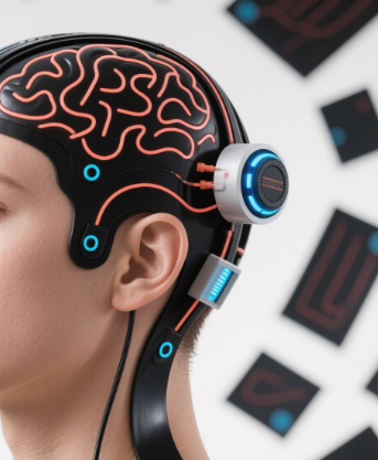
3. VR/AR Human–Computer Interaction
IV. Technical Challenges and Future Prospects
-
Environmental stability:
High-humidity environments (e.g., sweating, showering) may cause moisture absorption and swelling, leading to resistance drift of 10%–15%. Optimization via fluoride encapsulation or hydrophobic coatings is required.
-
Large-scale uniformity:
During large-area fabrication (>100 cm²), uneven distribution of conductive particles can result in resistance deviation of ±20%. Improved coating uniformity control in roll-to-roll processing is needed.
- Development of self-healing conductive films: Introduce dynamic covalent bonds or hydrogen bonds to achieve autonomous resistance recovery after mechanical damage (recovery rate >90%).
- Multi-sensing integration: Combine pressure, temperature, and humidity sensing in a single 100–200 kΩ conductive film, distinguishing multiple signals via different resistance responses.
- Low-power optimization: Integrate flexible integrated circuits to reduce power consumption of signal-acquisition circuits (mW level) and extend the battery life of wearable devices.