Optical Chip Bonding Adhesive
- Thermal Conductivity Coefficient: ≥1.5W/(m·K) for conventional scenarios; ≥3.0W/(m·K) for high-power scenarios (e.g., 100G+ optical modules)
- Thermal Resistance: ≤0.15℃·in²/W (when adhesive layer thickness is 50μm)
- Coefficient of Thermal Expansion (CTE): Shall match the CTE of chips (Si: ~3ppm/℃) and substrates (AlN: ~4.5ppm/℃), with a CTE difference ≤5ppm/℃ to avoid stress cracking under temperature cycling.
- Shear Strength: ≥15MPa (at 25℃), ≥8MPa (at 125℃)
- Tensile Strength: ≥20MPa; Elongation at Break: ≥5% (to prevent chip detachment under vibration and impact)
- Operating Temperature Range: -40℃~150℃ (covering the temperature range of high-power chips after heat dissipation)
- Damp-Heat Resistance: When stored at 85℃/85% RH for 1000h, the attenuation of thermal conductivity coefficient shall be ≤10%
- Thermal Shock Resistance: After 1000 cycles of -40℃ (30min) ↔125℃ (30min), there shall be no cracking or peeling of the adhesive layer.
- Epoxy-Based Thermal Conductive Adhesive: Suitable for medium and high-power scenarios, featuring fast curing speed (100℃/30min) and high bonding strength.
- Silicone-Based Thermal Conductive Adhesive: Suitable for ultra-high-power scenarios, with good flexibility and a wide CTE adjustment range, but relatively long curing time (150℃/60min).
- Filler Types: Silver powder (high thermal conductivity, high cost); Aluminum oxide (medium thermal conductivity, excellent cost-effectiveness); Aluminum nitride (high thermal conductivity + insulation, suitable for high-power chips requiring insulation).
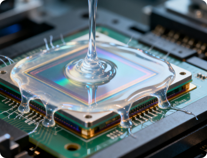
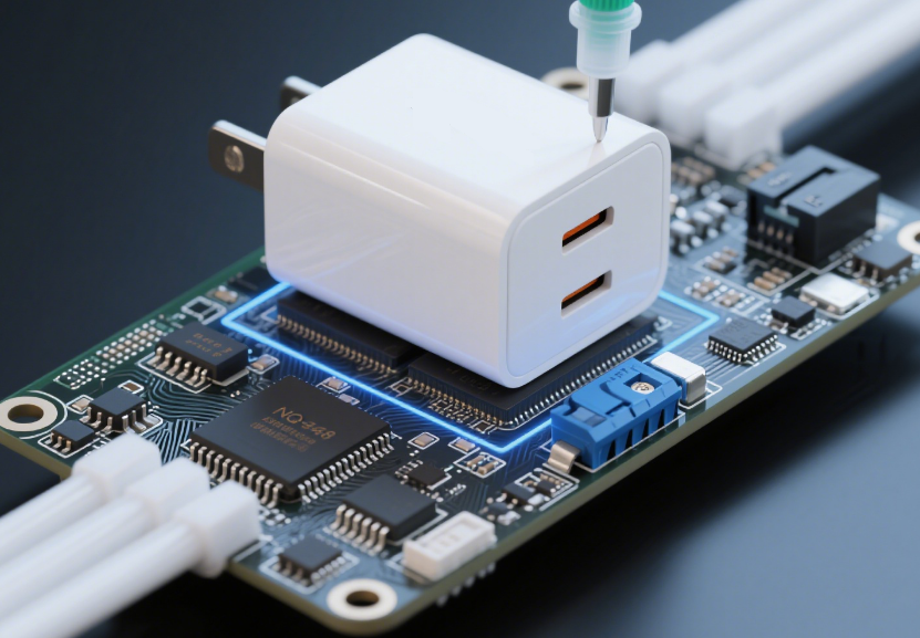
- Adhesive Application Method: Dispensing accuracy ±5%, adhesive layer thickness controlled between 30~80μm (excessive thickness affects thermal conductivity, while insufficient thickness easily causes gaps).
- Curing Atmosphere: Nitrogen protection is recommended (oxygen content ≤100ppm) to avoid oxidation and yellowing of the adhesive layer, which may affect heat dissipation.
- Volume Resistivity: ≥10¹⁴Ω·cm (at 25℃), ≥10¹²Ω·cm (at 85℃)
- Surface Resistivity: ≥10¹³Ω (at 25℃)
- Dielectric Constant: ≤3.5 (at 1MHz); Dielectric Loss: ≤0.005 (at 1MHz) (to avoid signal transmission interference)
- Curing Temperature: ≤80℃ (low-temperature curing type), ≤120℃ (medium-temperature curing type) (to avoid high-temperature damage to the chip PN junction)
- Curing Pressure: ≤50kPa (low-pressure process) (to prevent chip cracking, especially for brittle materials such as InP chips)
- Curing Time: ≤60min at 120℃, ≤120min at 80℃ (balancing production efficiency and chip protection)
- Ion Content: Cl⁻≤10ppm, Na⁺+K⁺≤5ppm (to avoid electrochemical corrosion of chip electrodes)
- Volatile Organic Compounds (VOC): ≤50ppm (at 150℃/1h) (to prevent volatile substances from adhering to the chip surface and affecting photoelectric performance)
- Modified Epoxy Adhesive: Low ion content and excellent insulation, suitable for most sensitive chips (e.g., radio frequency optical chips).
- Cyanate Ester Adhesive: Outstanding dielectric performance and strong damp-heat resistance, suitable for high-frequency sensitive chips (e.g., 5G optical module chips).
- Adhesive Layer Uniformity: Adopt jet dispensing technology, with adhesive layer thickness deviation ≤10% (to avoid local stress concentration).
- Curing Curve: Adopt stepwise temperature rise (e.g., 50℃/30min→80℃/60min) to reduce internal stress generation.
- Post-Treatment: After curing, a Post Cure at 120℃/2h is required to improve the stability of the adhesive layer.
- Ultrasonic Scanning (C-SAM): No voids with diameter ≥50μm (void ratio ≤5%)
- Push-Pull Test: Thrust ≥50N (for chips with size 1mm×1mm), no chip detachment or adhesive layer breakage.
- High-Temperature Storage: When stored at 150℃ for 1000h, the attenuation of insulation/thermal conductivity performance shall be ≤15%
- Temperature Cycling: After 1000 cycles of -40℃~125℃, there shall be no peeling between the adhesive layer and the chip/substrate.
