











blog

Material Properties and Applications of PDMS Membrane Sensing Chips

2026/07/21 0

I. Core Material Properties of PDMS Membranes for Sensing Chip Integration

1. Mechanical Properties (Core for Tactile / Pressure Sensing)

Tunable modulus: The standard 10:1 mixing ratio of prepolymer to curing agent yields a modulus of ~1.2 MPa; a low-crosslinking ratio of 30:1 reduces the modulus to tens of kPa, matching the mechanical properties of human skin and soft tissues. Its tensile breaking elongation exceeds 100%, with no cracking after repeated bending.

Microstructurability: Molding can replicate pyramid patterns, micropores, wrinkles and fingerprint microprotrusions to drastically boost pressure sensing sensitivity. Ultra-thin membranes (50–500 μm) deliver millisecond-scale deformation response.

2. Optical Properties (Mandatory for Optical Sensing Chips)

High transmittance across the full 240–1100 nm band with a refractive index of ~1.41 and zero fluorescence interference, compatible with SPR, SERS, optical fiber and fluorescence detection chips. After oxygen plasma treatment, PDMS can form permanent bonding with silicon wafers and glass to realize monolithic optoelectronic chip packaging (PMC).

3. Biochemical and Interfacial Properties (For Biosensing Chips)
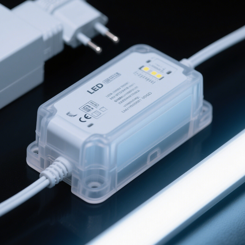
Material Properties and Applications of PDMS Membrane Sensing Chips插图

PDMS Thin-Film Sensing Chips

Non-cytotoxic and biocompatible, suitable for direct skin attachment or in-vivo implantation. Air, water and oxygen permeable, meeting requirements for cell culture and in-situ detection of sweat/body fluids.

Intrinsically hydrophobic; surface modification via oxygen plasma or Pluronic converts it to hydrophilicity to enable self-driven fluid flow in microfluidics. Au/Ag thin films can be sputtered on PDMS to fabricate flexible electrodes featuring high peel strength and stable conductivity under stretching.

4. Fabrication and Packaging Advantages

Low-cost molding via soft lithography; uniform ultra-thin films can be fabricated by spin-coating or blade-coating. Multi-layer PDMS can be plasma-bonded without adhesive or fluid leakage. Compatible with roll-to-roll mass production for batch manufacturing of large-area sensor arrays, cutting unit manufacturing costs by over 60%.

5. Tunable Permeation Properties (For Gas / Ion Sensing)

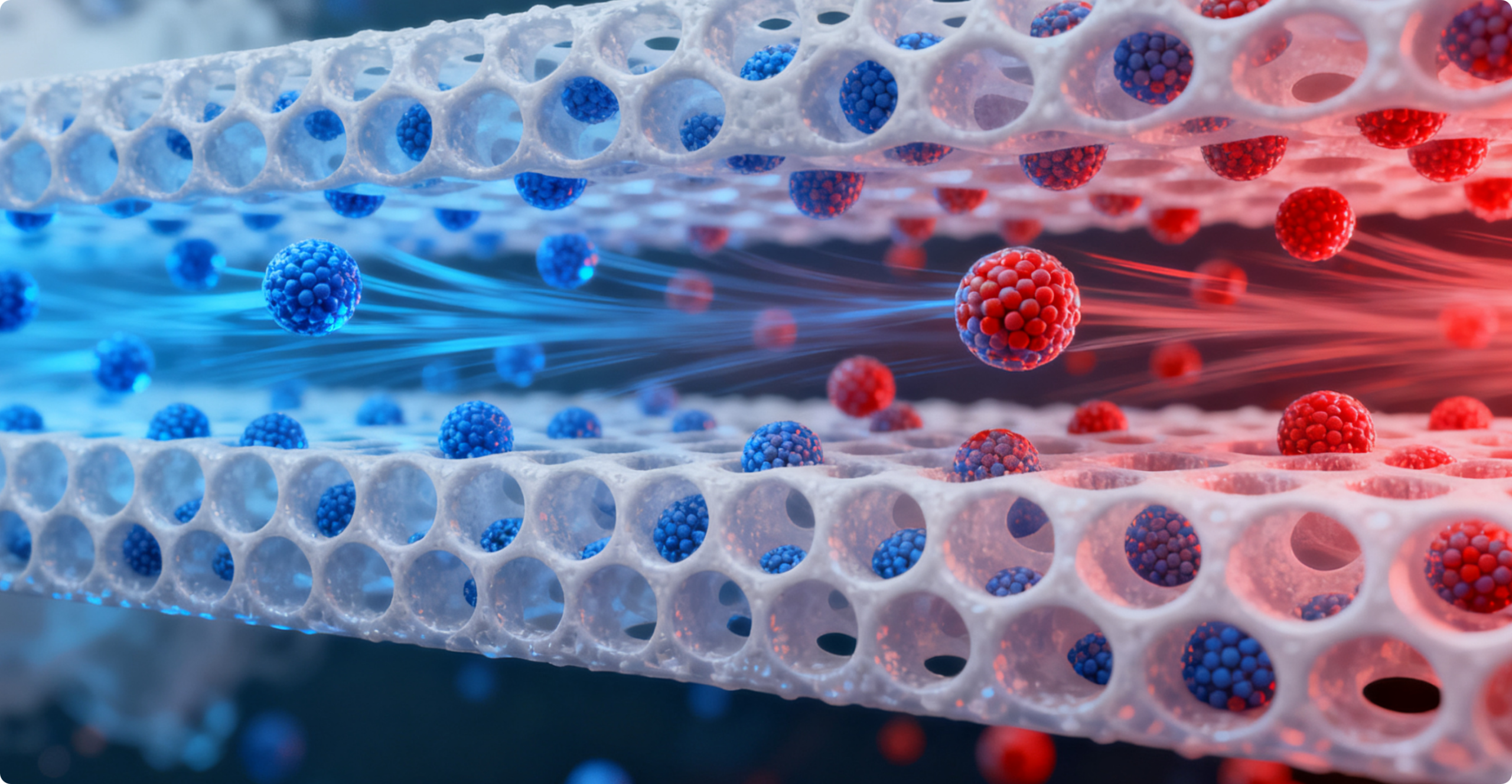
Small organic molecules, VOCs and water vapor selectively permeate PDMS membranes, while macromolecules and ions are blocked. PDMS acts as a breathable separation barrier to isolate electrolyte from the external environment while allowing target gases to diffuse toward electrode sensing regions.

II. Segmented Applications of PDMS Membranes in Various Electronic Sensing Chips

(I) Flexible Pressure / Tactile Sensing Chips (Electronic Skin, E-skin) — The Most Dominant Application

PDMS membranes serve as elastic dielectric layers or supporting substrates, categorized into two major chip architectures: capacitive and piezoresistive.

Capacitive Tactile Chips

Sandwich structure: two flexible metal electrodes (top and bottom) + microstructured PDMS dielectric film. Applied pressure compresses PDMS to narrow electrode spacing, resulting in a linear capacitance rise. Pyramid/hemispherical micropore structures introduce air gaps, lifting low-pressure sensitivity by more than 10 times, with a detection limit as low as 0.07 mN and response time < 1 ms.

Typical solution: GaN optoelectronic tactile chips coated with fingerprint-patterned PDMS films that mimic human epidermis, applied to organ tactile detection in minimally invasive surgery and sensor arrays for precision robotic grasping.

Structure of PDMS Bionic Tactile Chips

Piezoresistive Sensing Chips

Conductive elastic films are fabricated by blending PDMS with conductive fillers (carbon nanotubes, MXene, liquid metal). Compression alters the density of conductive pathways, generating resistance variation as output signals. Porous composite PDMS films achieve a measurement range up to 1275 kPa, covering fingertip micro-tactile perception, human pulse and plantar pressure monitoring chips.

Encapsulation Protective Layer

Ultra-thin PDMS encapsulates metal nanowire electrodes to isolate sweat and moisture, preventing oxidation and fracture of conductive layers and enabling long-term waterproof stable operation of wearable devices.

(II) Microfluidic Biochemical Sensing Chips (Lab-on-Chip, Sweat / Body Fluid Detection)

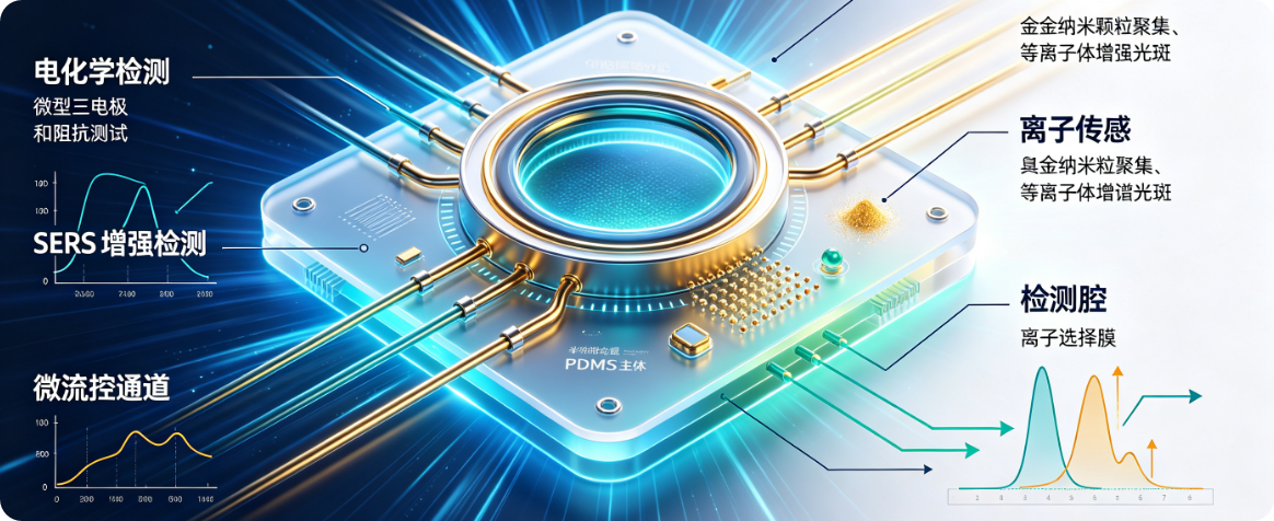
PDMS membranes form the primary structure of microfluidic chips, integrating electrochemical, SERS and ion sensing units.

Fluid Channel Layer

Soft lithography molds micron-scale microchannels, liquid reservoirs and filter cavities for precise manipulation of trace sweat, blood and cell fluid. Oxygen plasma bonding with silicon-based sensing electrode chips builds an integrated detection platform without external tubing.

Stacked Structure of PDMS Microfluidic Sweat Sensing Chips

Separation / Breathable Diaphragm

Ultra-thin PDMS films act as partition layers: microfluidic body fluid flows on one side, while silicon-based electrochemical electrodes reside on the other. Only small-molecule metabolites (lactic acid, urea, Na⁺, glucose) permeate the membrane, blocking interference from protein and cellular macromolecules to improve signal-to-noise ratio.

Encapsulation of Implantable On-Chip Electrodes

PDMS encapsulates miniature Ag/AgCl reference and working electrodes, offering biocompatibility and mechanical matching with in-vivo tissues. Composite Parylene coating suppresses water absorption and swelling to resolve baseline drift in physiological environments. Signal drift remains < 0.1 mmHg after 30 days of implantation, applicable to intracranial and vascular pressure sensing chips.

(III) Gas / VOC Sensing Chips (Fiber Optic, MOS, Electrochemical Gas-Sensitive Chips)

PDMS functions as a selective gas-permeable sensitive membrane. Core principle: organic gases exhibit distinct dissolution and diffusion rates in PDMS, enabling gas screening and enrichment.

Fiber-Optic SPR/VOC Chips

1–10 μm ultra-thin PDMS coatings are deposited on fiber sensing regions. Permeated VOCs swell PDMS and modify film refractive index, shifting fiber optical spectra for quantitative detection of formaldehyde, ethanol and benzene series, deployed in drunk driving screening and indoor air monitoring chips.

Protective Membranes for Metal Oxide Semiconductor (MOS) Gas-Sensitive Chips

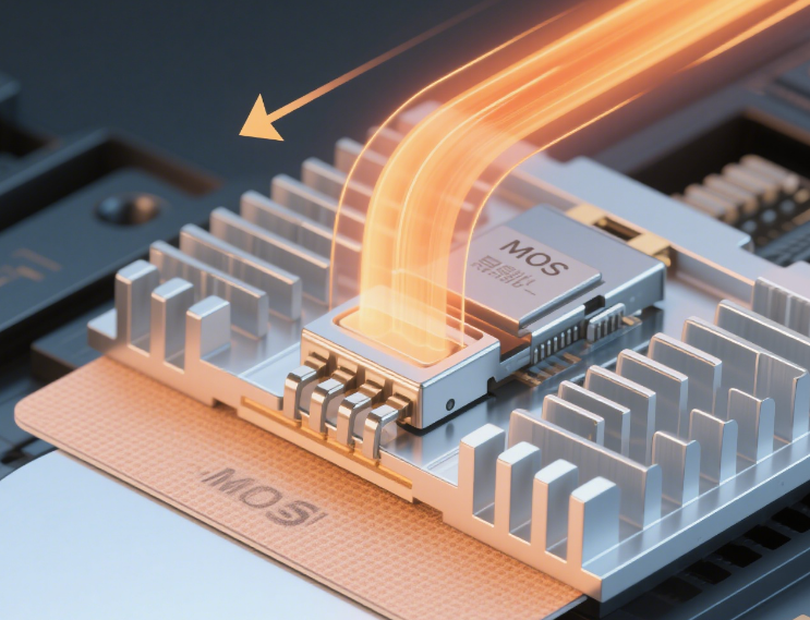
PDMS films cover MOS heating electrodes to block moisture and dust interference while transmitting target organic gases, mitigating humidity-induced zero drift of sensors. Porous modified PDMS accelerates gas penetration and shortens response time.

Breathable Diaphragms for Electrochemical Gas Sensors

Replaces traditional PTFE diaphragms; flexible enough to conform to miniature chips, prevents electrolyte leakage and allows CO, H₂S and O₂ to diffuse to catalytic electrodes, suitable for portable miniature gas detection chips.

(IV) Optoelectronic / SPR / SERS Optical Sensing Chips

Flexible Optical Substrates

PDMS flexible substrates replace rigid glass; gold nanofilm sputtering on PDMS produces SPR sensing chips. The substrates can bend to fit curved samples without attenuation of refractive index detection sensitivity after repeated bending, used for flexible optical detection of food alcohol and biomolecules.

Sealing Layers for SERS Enhancement Cavities

PDMS covers gold nanostructured SERS chips to form closed microcavities where target molecules are enriched, amplifying Raman signals by 10⁶ times to realize single-molecule trace biochemical detection. High light transmittance permits laser penetration for signal excitation and collection.

(V) Wearable Physiological Electrical Sensing Chips (ECG, EMG, EEG)

Flexible Substrates

Ultra-thin PDMS films support Au / liquid metal flexible electrodes with skin-matched modulus, delivering non-irritating wear experience and tight epidermal adhesion during movement to reduce motion artifact noise.

Ion Channel Buffer Layer

Ionic liquid-doped PDMS gel films serve as electrode-skin interfaces to stabilize contact potential and enhance signal acquisition stability for ECG and EMG, applied to flexible patch-type cardiac monitoring chips.

III. Standard Fabrication of PDMS Films and Chip Integration Processes

Film Preparation

Mix Sylgard 184 prepolymer and curing agent at a 10:1 ratio, followed by vacuum degassing for 45–60 min to eliminate air bubbles. Toluene dilution enables micron-scale ultra-thin coating fabrication.

Film Forming Methods

  • Spin-coating: 500–3000 rpm, film thickness 10–200 μm with high uniformity, compatible with wafer-level sensing chips;
  • Blade-coating / Casting: Molded thick films (200 μm–2 mm) for microfluidic channels and tactile dielectric layers;
  • Dip-coating: Ultra-thin gas-sensitive coatings on fiber end faces.

Curing Conditions

  • Complete crosslinking: Baking at 60–65 °C for 2 h;
  • Fast curing: 110 °C for 1.5 h;
  • Slow room-temperature curing (24 h): Delivers higher film elasticity.

Chip Bonding (Core Integration Step)

PDMS films and silicon/glass sensing chips are activated via oxygen plasma (40 W, 45 s) to generate surface hydroxyl groups. Irreversible covalent bonding forms under room-temperature pressure without adhesive or fluid leakage, serving as the standardized process for microfluidic sensing chips.

Surface Modification for Functional Expansion

  • Oxygen plasma: Convert hydrophobic surface to hydrophilicity for self-driven microfluidic flow;
  • Gold / titanium sputtering: Fabricate on-chip flexible electrodes;
  • Parylene vapor deposition: Form dense waterproof barriers to resolve water absorption drift of implanted devices;
  • Conductive filler doping: Manufacture piezoresistive elastic sensing films.

IV. Inherent Technical Limitations and Chip-Level Optimization Strategies

1. Intrinsic Drawbacks

  1. Inherent hydrophobicity tends to adsorb organic substances, causing non-specific adsorption interference in biochemical detection;
  2. Water vapor and polar small molecules readily permeate PDMS, leading to film swelling and sensing baseline drift under high temperature or long-term immersion;
  3. Low insulating dielectric constant (ε ≈ 2.7) caps the maximum sensitivity of pure PDMS capacitive sensors;
  4. Poor resistance to strongly polar solvents (acetone, high-concentration ethanol), causing swelling and deformation of microfluidic organic detection channels.

2. Engineering Optimization Solutions

  • Composite modification: Dope PDMS with high-dielectric BaTiO₃ particles to boost capacitive sensing sensitivity; porous/Parylene composite double-layer films block moisture penetration;
  • Surface functionalization: Pluronic and hydrophilic coatings reduce protein adsorption;
  • Ratio regulation: Increase curing agent proportion to raise crosslink density and mitigate swelling;
  • Composite encapsulation: PDMS + PI / epoxy composite layers balance flexibility and barrier performance for industrial and implantable high-precision sensing chips.

V. Industrial Application Scenarios and Development Trends

Application Scenarios

  • Healthcare & Medical: Wearable sweat biochemical patches, tactile sensors for minimally invasive surgery, implantable intracranial pressure monitoring chips, flexible ECG electrodes;
  • Robotics & Human-Machine Interaction: Electronic skin tactile arrays, force perception chips for bionic manipulators;
  • Environmental Monitoring: Miniature fiber-optic VOC sensors, portable toxic gas detection chips;
  • Biological Laboratories: Organ-on-Chip cell microfluidic sensing, high-throughput biochemical detection chips;
  • Consumer Electronics: Curved screen touch sensing, flexible wristband pressure & pulse detection chips.

Future Development Directions

  1. Functionally integrated PDMS: Monolithic conductive, gas-sensitive and ion-selective thin films enabling simultaneous multi-parameter detection on single chips;
  2. Ultra-thin nanoscale PDMS coatings for miniature MEMS and chip-scale packaged micro gas-sensitive devices;
  3. Degradable modified PDMS for disposable short-term implantable sensing chips to avoid secondary surgical removal;
  4. Large-area roll-to-roll mass production of PDMS flexible sensor arrays to cut commercialization costs of wearable chips;
  5. High-barrier composite PDMS films to address long-term stability bottlenecks of implantable and industrial high-temperature/high-humidity applications.
Advisory Message
Leave your needs and contact information,we will communicate with you in time
Contact Us